- 您现在的位置:买卖IC网 > Sheet目录286 > 24C08B-E/P (Microchip Technology)IC EEPROM 8KBIT 100KHZ 8DIP
�� �
�
�24C08B/16B�
�2.0�
�FUNCTIONAL� DESCRIPTION�
�3.4�
�Data Valid (D)�
�The� 24C08B/16B� supports� a� Bi-directional� 2-wire� bus�
�and� data� transmission� protocol.� A� device� that� sends�
�data� onto� the� bus� is� defined� as� transmitter,� and� a�
�device� receiving� data� as� receiver.� The� bus� has� to� be�
�controlled� by� a� master� device� which� generates� the�
�serial� clock� (SCL),� controls� the� bus� access,� and� gener-�
�ates� the� START� and� STOP� conditions,� while� the�
�24C08B/16B� works� as� slave.� Both,� master� and� slave�
�can� operate� as� transmitter� or� receiver� but� the� master�
�device� determines� which� mode� is� activated.�
�The� state� of� the� data� line� represents� valid� data� when,�
�after� a� START� condition,� the� data� line� is� stable� for� the�
�duration� of� the� HIGH� period� of� the� clock� signal.�
�The� data� on� the� line� must� be� changed� during� the� LOW�
�period� of� the� clock� signal.� There� is� one� clock� pulse� per�
�bit� of� data.�
�Each� data� transfer� is� initiated� with� a� START� condition�
�and� terminated� with� a� STOP� condition.� The� number� of�
�the� data� bytes� transferred� between� the� START� and�
�3.0�
�BUS� CHARACTERISTICS�
�STOP� conditions� is� determined� by� the� master� device�
�and� is� theoretically� unlimited,� although� only� the� last� 16�
�The� following� bus� protocol� has� been� defined:�
�?� Data� transfer� may� be� initiated� only� when� the� bus�
�is� not� busy.�
�will� be� stored� when� doing� a� write� operation.� When� an�
�overwrite� does� occur� it� will� replace� data� in� a� first� in� first�
�out� fashion.�
�?� During� data� transfer,� the� data� line� must� remain�
�stable� whenever� the� clock� line� is� HIGH.� Changes�
�3.5�
�Acknowledge�
�in� the� data� line� while� the� clock� line� is� HIGH� will� be�
�interpreted� as� a� START� or� STOP� condition.�
�Accordingly,� the� following� bus� conditions� have� been�
�defined� (Figure� 3-1).�
�Each� receiving� device,� when� addressed,� is� obliged� to�
�generate� an� acknowledge� after� the� reception� of� each�
�byte.� The� master� device� must� generate� an� extra� clock�
�pulse� which� is� associated� with� this� acknowledge� bit.�
�3.1�
�Bus not Busy (A)�
�Note:�
�The� 24C08B/16B� does� not� generate� any�
�acknowledge� bits� if� an� internal� program-�
�Both� data� and� clock� lines� remain� HIGH.�
�ming� cycle� is� in� progress.�
�The� device� that� acknowledges,� has� to� pull� down� the�
�3.2�
�Start Data Transfer (B)�
�SDA� line� during� the� acknowledge� clock� pulse� in� such� a�
�A� HIGH� to� LOW� transition� of� the� SDA� line� while� the�
�clock� (SCL)� is� HIGH� determines� a� START� condition.�
�All� commands� must� be� preceded� by� a� START� condi-�
�tion.�
�way� that� the� SDA� line� is� stable� LOW� during� the� HIGH�
�period� of� the� acknowledge� related� clock� pulse.� Of�
�course,� setup� and� hold� times� must� be� taken� into�
�account.� During� reads,� a� master� must� signal� an� end� of�
�data� to� the� slave� by� NOT� generating� an� acknowledge�
�3.3�
�Stop Data Transfer (C)�
�bit� on� the� last� byte� that� has� been� clocked� out� of� the�
�slave.� In� this� case,� the� slave� (24C08B/16B)� will� leave�
�A� LOW� to� HIGH� transition� of� the� SDA� line� while� the�
�clock� (SCL)� is� HIGH� determines� a� STOP� condition.� All�
�operations� must� be� ended� with� a� STOP� condition.�
�the� data� line� HIGH� to� enable� the� master� to� generate� the�
�STOP� condition.�
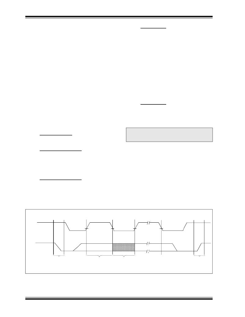
�FIGURE� 3-1:�
�DATA� TRANSFER� SEQUENCE� ON� THE� SERIAL� BUS�
�(A)�
�(B)�
�(D)�
�(D)�
�(C)�
�(A)�
�SCL�
�SDA�
�START�
�CONDITION�
�ADDRESS� OR�
�ACKNOWLEDGE�
�DATA�
�ALLOWED�
�STOP�
�CONDITION�
�DS21081G-page� 4�
�VALID�
�TO� CHANGE�
�?� 2004� Microchip� Technology� Inc.�
�发布紧急采购,3分钟左右您将得到回复。
相关PDF资料
24FC1026-I/P
IC EEPROM 1024KB 1MHZ 8-DIP
24FC128-I/MNY
IC EEPROM 128KBIT 1MHZ 8TDFN
24FC515T-I/SM
IC EEPROM 512KBIT 1MHZ 8SOIC
24FC64T-I/MF
IC EEPROM 64KBIT 1MHZ 8DFN
24LC014H-I/P
IC EEPROM 1KBIT 400KHZ 8DIP
24LC014T-E/OT
IC EEPROM 1KBIT 400KHZ SOT23-6
24LC01B-I/SNG
IC EEPROM 1KBIT 400KHZ 8SOIC
24LC024H-I/ST
IC EEPROM 2KBIT 400KHZ 8TSSOP
相关代理商/技术参数
24C08B-E/SL
制造商:未知厂家 制造商全称:未知厂家 功能描述:I2C Serial EEPROM
24C08B-E/SN
制造商:未知厂家 制造商全称:未知厂家 功能描述:I2C Serial EEPROM
24C08B-EP
制造商:MICROCHIP 制造商全称:Microchip Technology 功能描述:8K/16K 5.0V I 2 C O Serial EEPROMs
24C08B-ESL
制造商:MICROCHIP 制造商全称:Microchip Technology 功能描述:8K/16K 5.0V I 2 C O Serial EEPROMs
24C08B-ESN
制造商:MICROCHIP 制造商全称:Microchip Technology 功能描述:8K/16K 5.0V I 2 C O Serial EEPROMs
24C08B-I/P
制造商:未知厂家 制造商全称:未知厂家 功能描述:I2C Serial EEPROM
24C08B-I/SL
制造商:未知厂家 制造商全称:未知厂家 功能描述:I2C Serial EEPROM
24C08B-I/SN
制造商:未知厂家 制造商全称:未知厂家 功能描述:I2C Serial EEPROM